- 您现在的位置:买卖IC网 > Sheet目录2008 > MAX1184ECM+TD (Maxim Integrated Products)IC ADC 10BIT 20MSPS DL 48-TQFP
MAX1184
Dual 10-Bit, 20Msps, 3V, Low-Power ADC with
Internal Reference and Parallel Outputs
______________________________________________________________________________________
13
Clock Input (CLK)
The MAX1184’s CLK input accepts CMOS-compatible
clock signals. Since the interstage conversion of the
device depends on the repeatability of the rising and
falling edges of the external clock, use a clock with low
jitter and fast rise and fall times (< 2ns). In particular,
sampling occurs on the rising edge of the clock signal,
requiring this edge to provide lowest possible jitter. Any
significant aperture jitter would limit the SNR perfor-
mance of the on-chip ADCs as follows:
where fIN represents the analog input frequency and tAJ
is the time of the aperture jitter.
Clock jitter is especially critical for undersampling
applications. The clock input should always be consid-
ered as an analog input and routed away from any ana-
log input or other digital signal lines.
The MAX1184 clock input operates with a voltage thresh-
old set to VDD/2. Clock inputs with a duty cycle other than
50%, must meet the specifications for high and low peri-
ods as stated in the Electrical Characteristics.
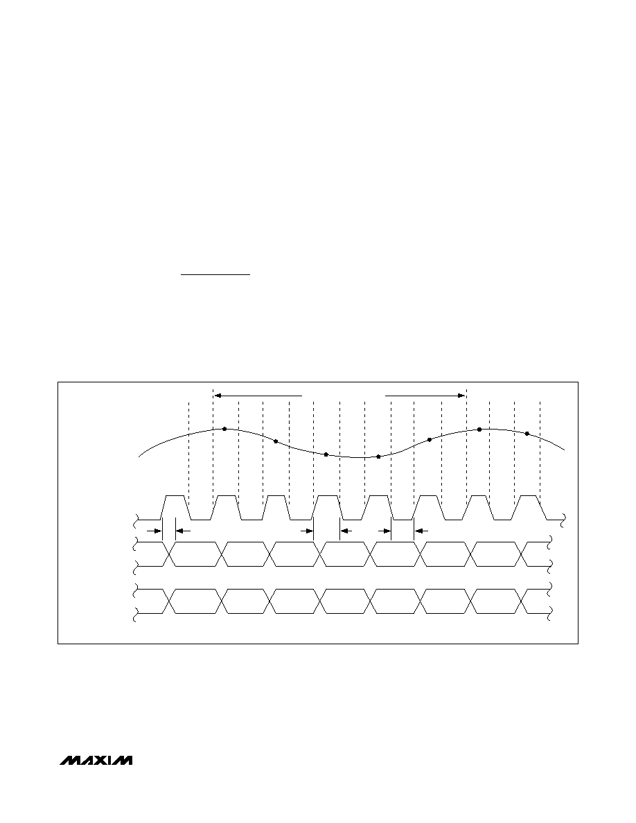
System Timing Requirements
Figure 3 depicts the relationship between the clock
input, analog input, and data output. The MAX1184
samples at the rising edge of the input clock. Output
data for channels A and B is valid on the next rising
edge of the input clock. The output data has an internal
latency of five clock cycles. Figure 4 also determines
the relationship between the input clock parameters
and the valid output data on channels A and B.
Digital Output Data, Output Data Format
Selection (T/B), Output Enable (
OE)
All digital outputs, D0A–D9A (Channel A) and
D0B–D9B (Channel B), are TTL/CMOS logic-compati-
ble. There is a five-clock-cycle latency between any
particular sample and its corresponding output data.
SNR
ft
IN
AJ
=×
××
×
20
1
2
log
)
π
N - 6
N
N - 5
N + 1
N - 4
N + 2
N - 3
N + 3
N - 2
N + 4
N - 1
N + 5
N
N + 6
N + 1
5-CLOCK-CYCLE LATENCY
ANALOG INPUT
CLOCK INPUT
DATA OUTPUT
D9A–D0A
tDO
tCH
tCL
N - 6
N - 5
N - 4
N - 3
N - 2
N - 1
N
N + 1
DATA OUTPUT
D9B–D0B
Figure 3. System Timing Diagram
发布紧急采购,3分钟左右您将得到回复。
相关PDF资料
MAX1186ECM+TD
IC ADC 10BIT 40MSPS DL 48-TQFP
MAX1187CCUI+
IC ADC 16BIT 135KSPS 28-TSSOP
MAX118EAI+
IC ADC 8BIT 1MSPS 28-SSOP
MAX1191ETI+T
IC ADC 8BIT 7.5MSPS DL 28-TQFN
MAX1192ETI+T
IC ADC 8BIT 22MSPS DL 28-TQFN
MAX1195ECM+TD
IC ADC 8BIT 40MSPS DL 48-TQFP
MAX1197ECM+TD
IC ADC 8BIT 60MSPS DL 48-TQFP
MAX1202AEPP+
IC ADC 12BIT 8CH 20-DIP
相关代理商/技术参数
MAX1184ECM-D
功能描述:模数转换器 - ADC RoHS:否 制造商:Texas Instruments 通道数量:2 结构:Sigma-Delta 转换速率:125 SPs to 8 KSPs 分辨率:24 bit 输入类型:Differential 信噪比:107 dB 接口类型:SPI 工作电源电压:1.7 V to 3.6 V, 2.7 V to 5.25 V 最大工作温度:+ 85 C 安装风格:SMD/SMT 封装 / 箱体:VQFN-32
MAX1184ECM-T
制造商:Maxim Integrated Products 功能描述:DUAL 10-BIT, 20MSPS, +3V, LOW-POWER ADC WITH - Tape and Reel
MAX1184ECM-TD
功能描述:模数转换器 - ADC RoHS:否 制造商:Texas Instruments 通道数量:2 结构:Sigma-Delta 转换速率:125 SPs to 8 KSPs 分辨率:24 bit 输入类型:Differential 信噪比:107 dB 接口类型:SPI 工作电源电压:1.7 V to 3.6 V, 2.7 V to 5.25 V 最大工作温度:+ 85 C 安装风格:SMD/SMT 封装 / 箱体:VQFN-32
MAX11850ETM+
功能描述:触摸屏转换器和控制器
RoHS:否 制造商:Microchip Technology 类型:Resistive Touch Controllers 输入类型:3 Key 数据速率:140 SPS 分辨率:10 bit 接口类型:4-Wire, 5-Wire, 8-Wire, I2C, SPI 电源电压:2.5 V to 5.25 V 电源电流:17 mA 工作温度:- 40 C to + 85 C 封装 / 箱体:SSOP-20
MAX11850ETM+T
功能描述:触摸屏转换器和控制器
RoHS:否 制造商:Microchip Technology 类型:Resistive Touch Controllers 输入类型:3 Key 数据速率:140 SPS 分辨率:10 bit 接口类型:4-Wire, 5-Wire, 8-Wire, I2C, SPI 电源电压:2.5 V to 5.25 V 电源电流:17 mA 工作温度:- 40 C to + 85 C 封装 / 箱体:SSOP-20
MAX11850GTM+
功能描述:触摸屏转换器和控制器
RoHS:否 制造商:Microchip Technology 类型:Resistive Touch Controllers 输入类型:3 Key 数据速率:140 SPS 分辨率:10 bit 接口类型:4-Wire, 5-Wire, 8-Wire, I2C, SPI 电源电压:2.5 V to 5.25 V 电源电流:17 mA 工作温度:- 40 C to + 85 C 封装 / 箱体:SSOP-20
MAX11850GTM+T
功能描述:触摸屏转换器和控制器
RoHS:否 制造商:Microchip Technology 类型:Resistive Touch Controllers 输入类型:3 Key 数据速率:140 SPS 分辨率:10 bit 接口类型:4-Wire, 5-Wire, 8-Wire, I2C, SPI 电源电压:2.5 V to 5.25 V 电源电流:17 mA 工作温度:- 40 C to + 85 C 封装 / 箱体:SSOP-20
MAX11850HTEVS+
功能描述:数据转换 IC 开发工具 RoHS:否 制造商:Texas Instruments 产品:Demonstration Kits 类型:ADC 工具用于评估:ADS130E08 接口类型:SPI 工作电源电压:- 6 V to + 6 V